Our Mission and Scope
Our Mission and Scope
Breaking AI's "Power Wall" for sustainable semiconductor innovation.
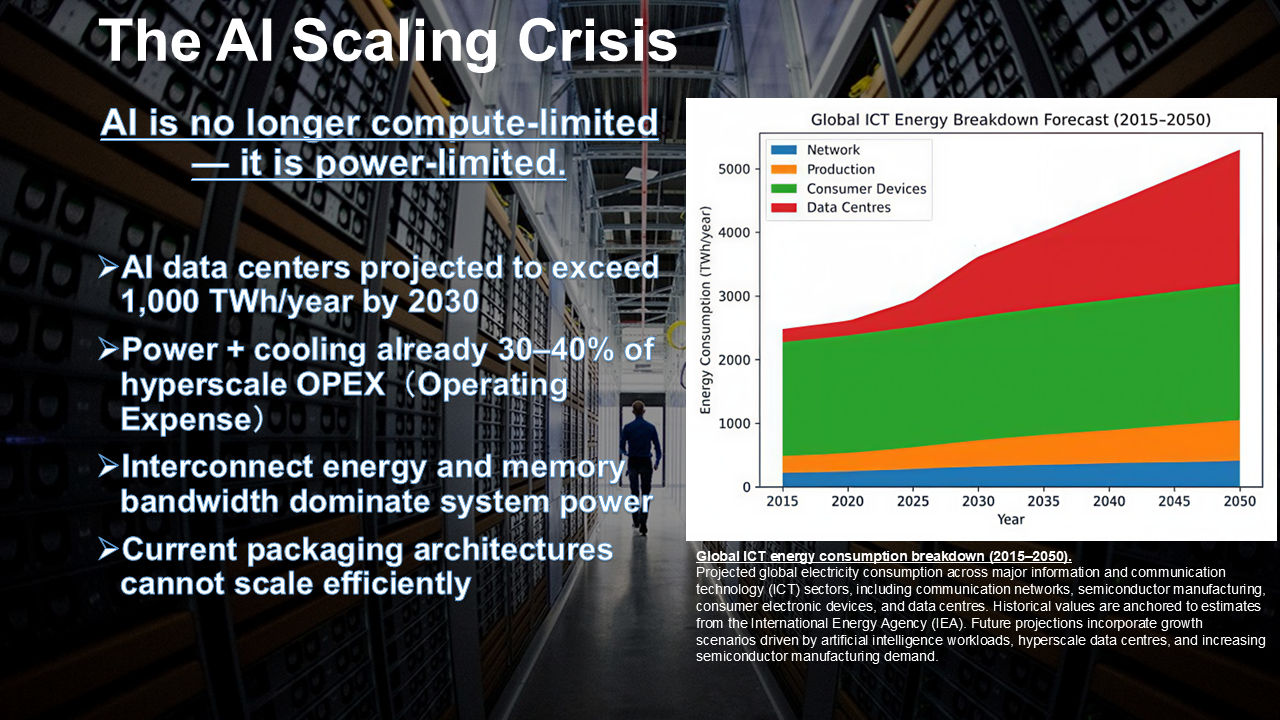
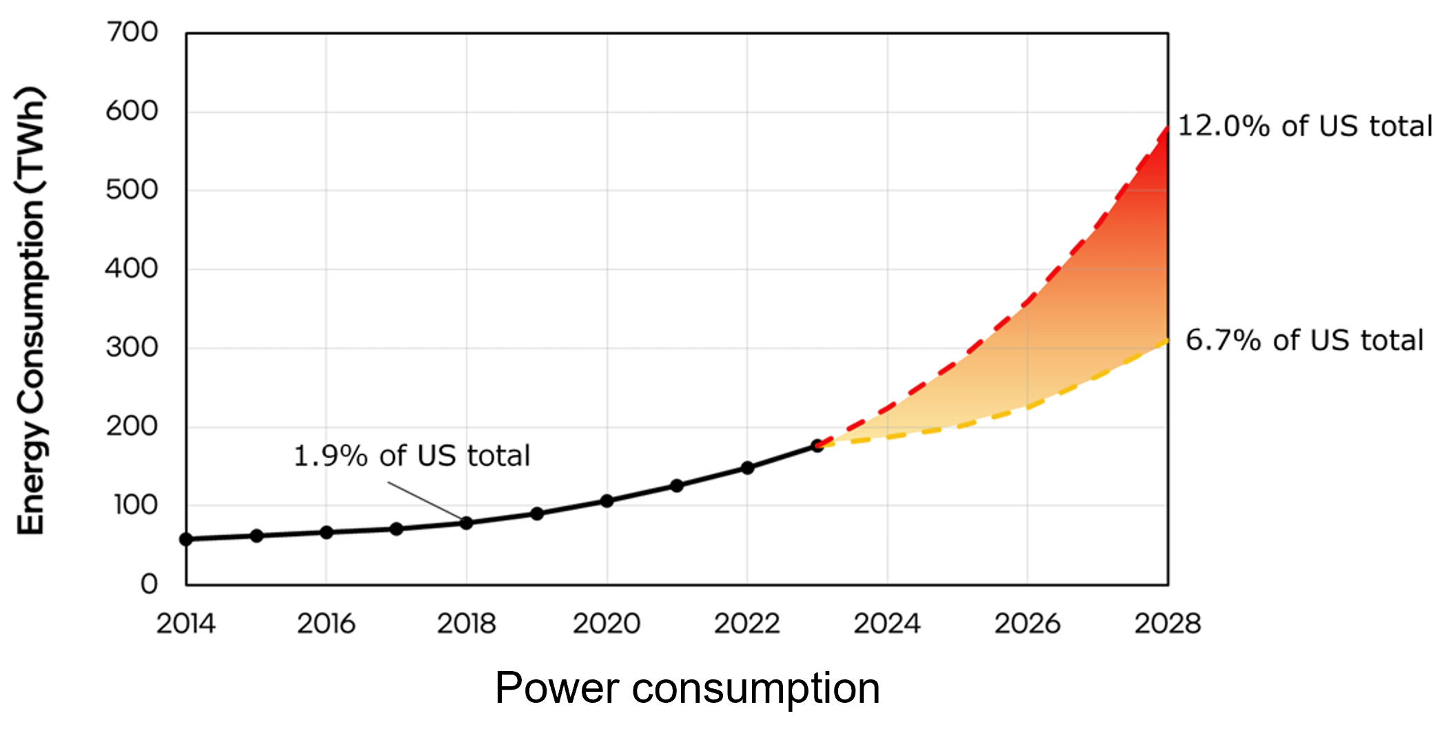
AI is currently facing a "power wall" rather than a limit in computing power. Forecasts suggest AI data center energy use will exceed 1,000 TWh by 2030. Already, power and cooling account for 30–40% of operational costs, while grid constraints are delaying the expansion of hyperscale data centers.
Solving these bottlenecks and improving energy efficiency is essential for continued AI growth.
At our core is Deep Tech IP protected by international patents. We are redefining the "Performance-per-Watt" curve to achieve the following:
◆ Achieving up to a 1,000x reduction in power consumption, depending on the architecture.
◆ Realizing an approximately 50% reduction in heat generation.
◆ Establishing innovative interconnect and integration technologies.
This is not merely an incremental optimization; it is a structural shift that will change the very economics of AI infrastructure.
The next leap in AI will not come from more computing power, but from dramatically higher energy efficiency. We aim to lead this transformation.
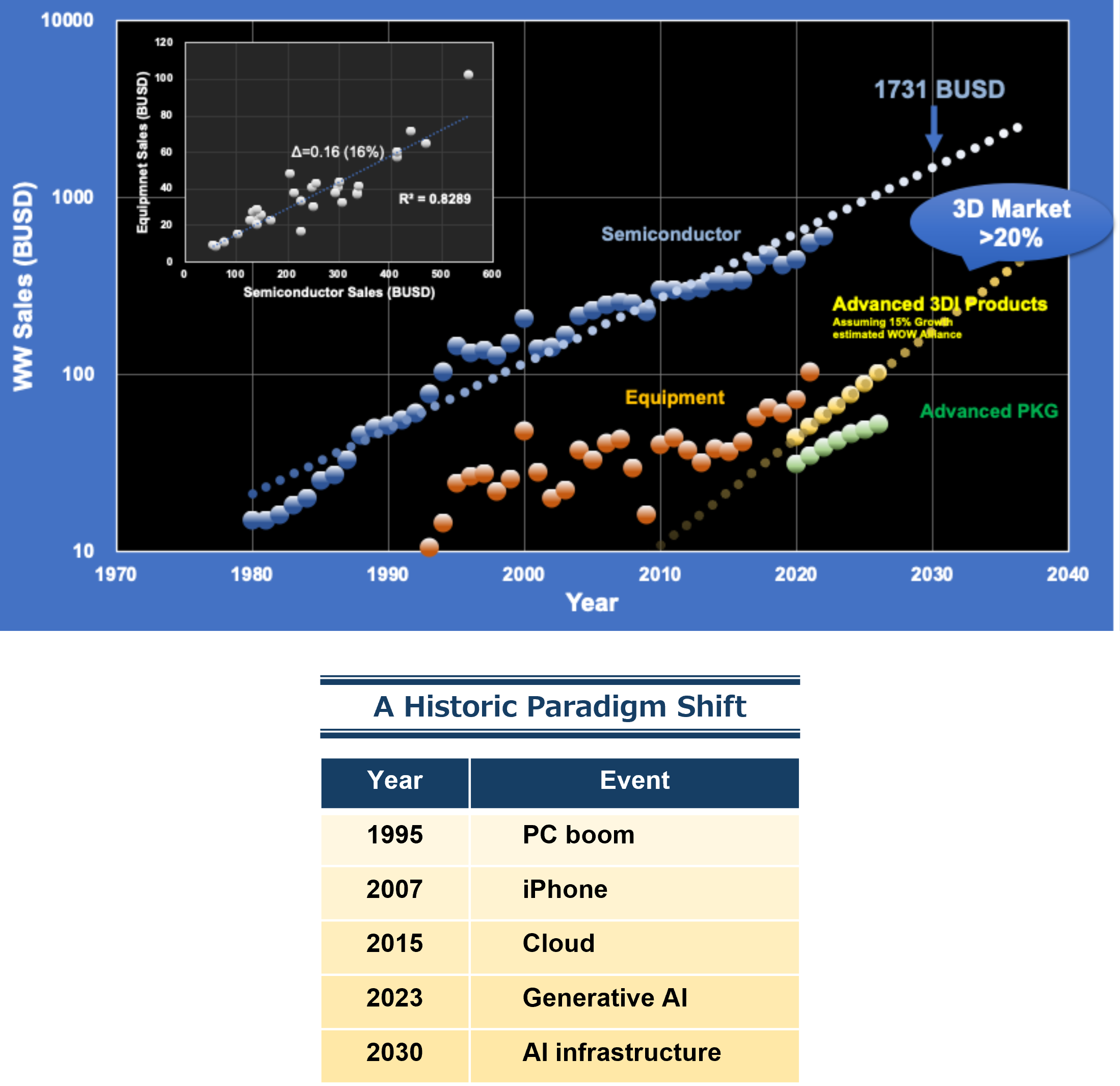
Opening the frontier in advanced packaging for a $1.7 trillion market.
The semiconductor market is at a structural turning point, projected to reach $1.7 trillion by 2030.
AI accelerators are currently the fastest-growing segment, and advanced packaging is becoming the new frontier in the competition for performance. In this era of transformation, energy-efficient architecture will be the key factor that determines the next winners.
Liberating AI from structural bottlenecks.
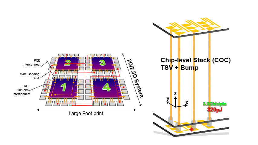
Current AI systems are held back by the physical limits of conventional packaging. Challenges such as long wiring distances, high parasitic capacitance, and thermal density limits create significant barriers to cost and yield in large-scale systems.
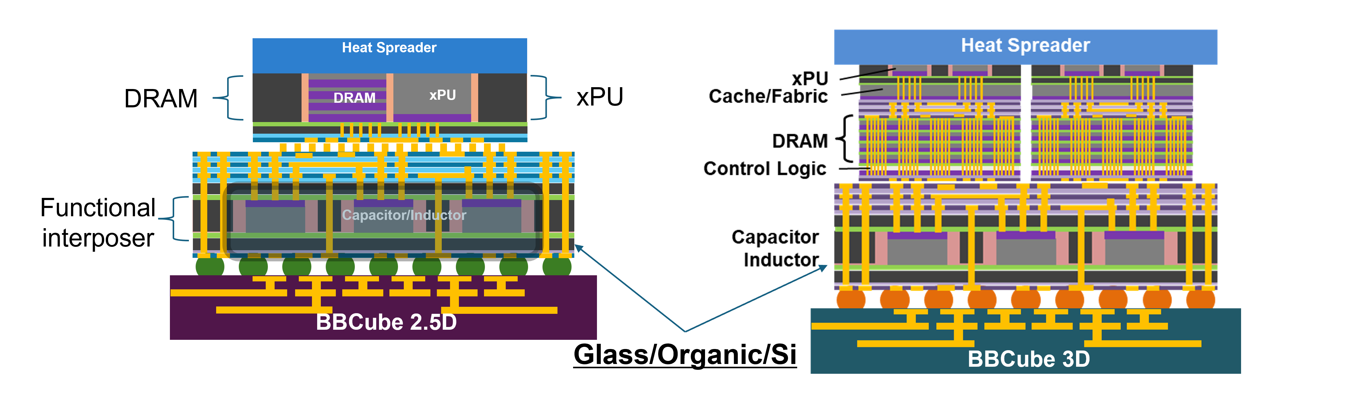
We break free from the traditional "side-by-side" approach. By utilizing Chip-on-Chip (CoC) stacking and other advanced techniques, we reduce wiring resistance and energy loss, effectively resolving these structural bottlenecks.
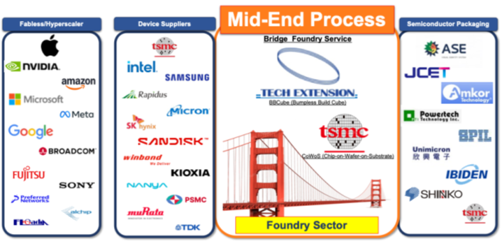
A "Bridge Foundry" connecting academia and industry: An ecosystem for accelerated co-creation.
Tech Extension (TEX) is driving the commercialization of BBCube technology.
With BBCube technology—born from research at the Institute of Science Tokyo—as our pillar, we are building a "Bridge Foundry" model. Through close partnerships within the WOW Alliance ecosystem (equipment, materials, and device partners), we connect fabless companies, hyperscalers, and OSATs.
◆ For more details on BBCube technology, please visit our Technology page.
We are scheduled to begin production through our Bridge Foundry in 2026.
Business Opportunity: Establishing Energy-Efficient Architecture for the AI Era
We are building the infrastructure layer for sustainable AI computing, enabling the realization of next-generation AI chips.
Through partnerships with hyperscalers and AI chip companies, we are driving our business forward, targeting the advanced 3D semiconductor integration market.
Our Vision for the Future:
With BBCube, we will establish the energy-efficient architecture essential for the AI era and create new business value.