Technology introduction
TECH EXTENSION Utilize the results of the Ohba Laboratory, WOW Alliance Heterogeneous and Functional Integration Unit,
Institute of Innovative Research, Science Tokyo.
Learn more about the technology. Website of Ohba Lab. [Crick here]
Our Breakthrough : BBCube
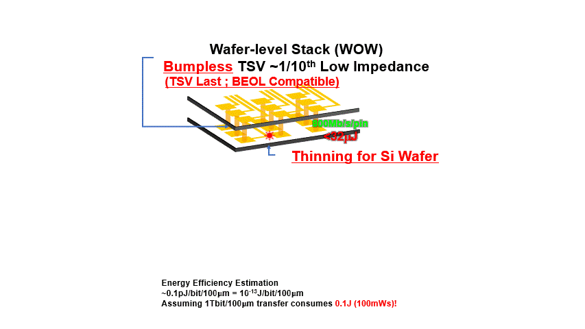
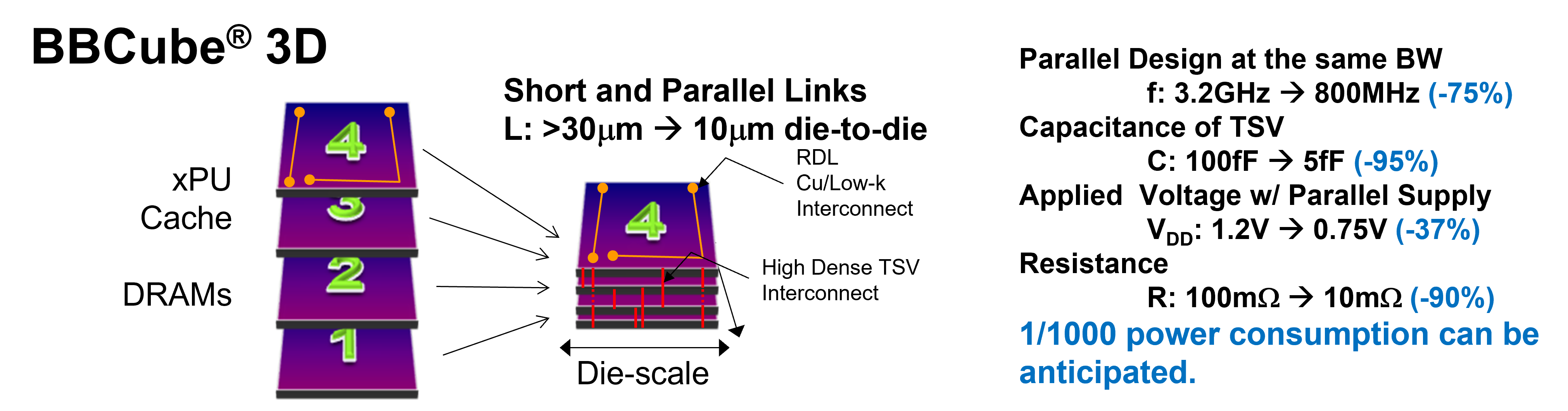
BBCube (Bumpless Build Cube) is a next-generation 3D architecture that is paving the way for the future of semiconductors.
Developed through the collective expertise of the "WOW Alliance" at the Tokyo Institute of Technology (now Institute of Science Tokyo), this innovative technology achieves a high-level integration of Wafer-on-Wafer (WOW) and Chip-on-Wafer (COW).
By leveraging an ultimate stacking structure featuring ultra-thin wafers and high-density TSV interconnects, we enable a new dimension of performance through micron-level device proximity.
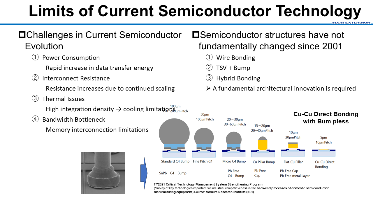
This technology represents a true breakthrough, shattering the structural constraints of the past.
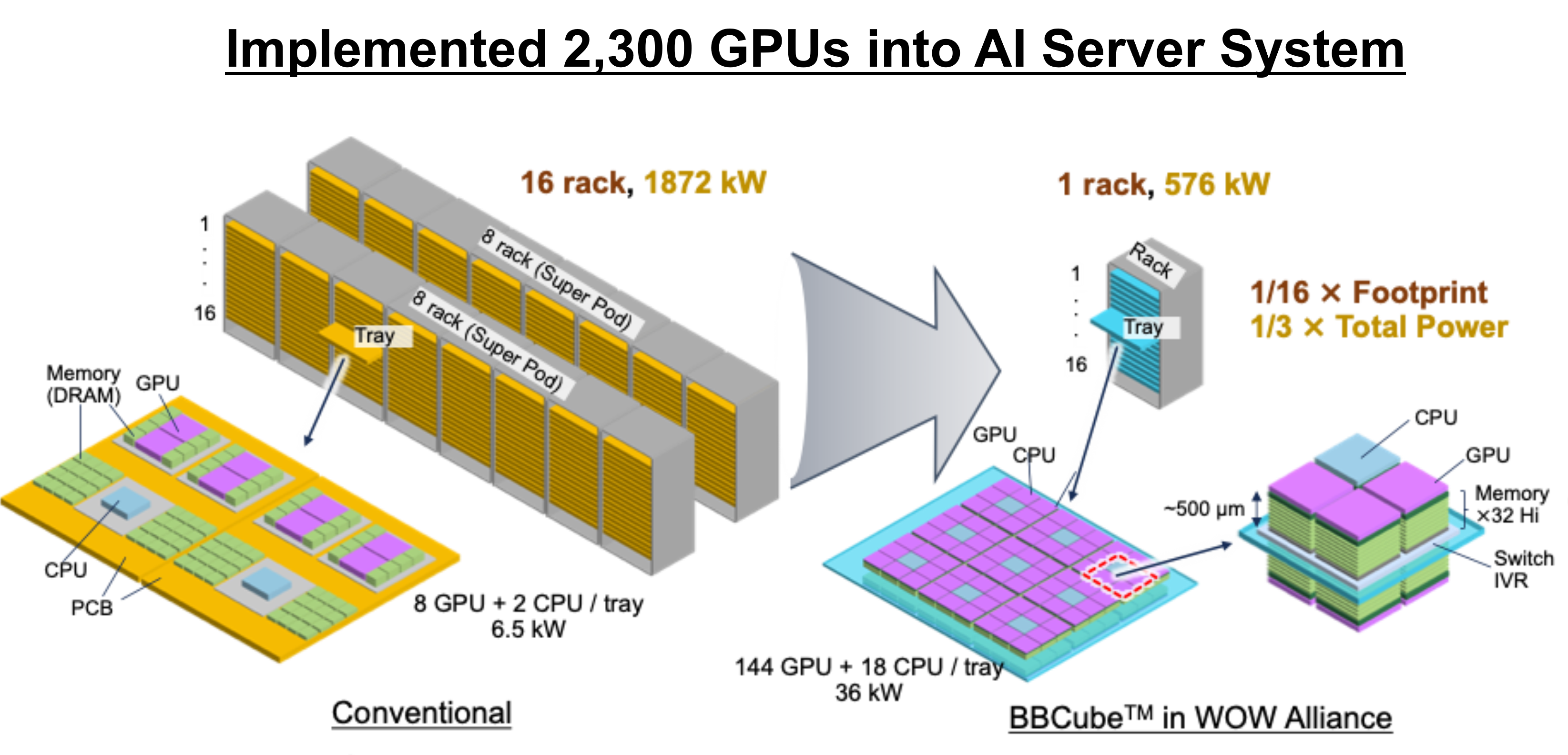
An overwhelming 10× to 1000× efficiency gain, driven by the structural innovation of BBCube.
BBCube dramatically boosts system efficiency, delivering the following "Five Value Propositions" that shatter conventional structural constraints.
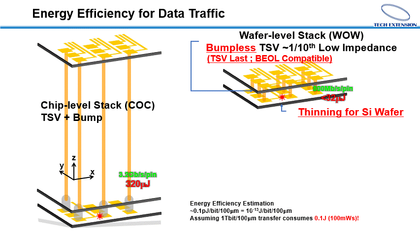
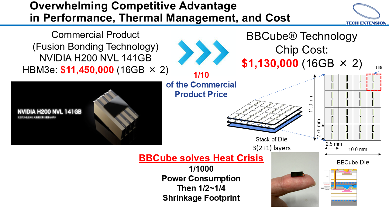
◆ Reducing interconnect power consumption by up to 1/1000.
◆ Reducing heat generation by approximately 50%.
◆ Shrinking the system footprint to 1/2–1/4 of its original size.
◆ Achieving overwhelmingly low-impedance connectivity.
◆ Enabling massively parallel I/O optimized for AI systems.
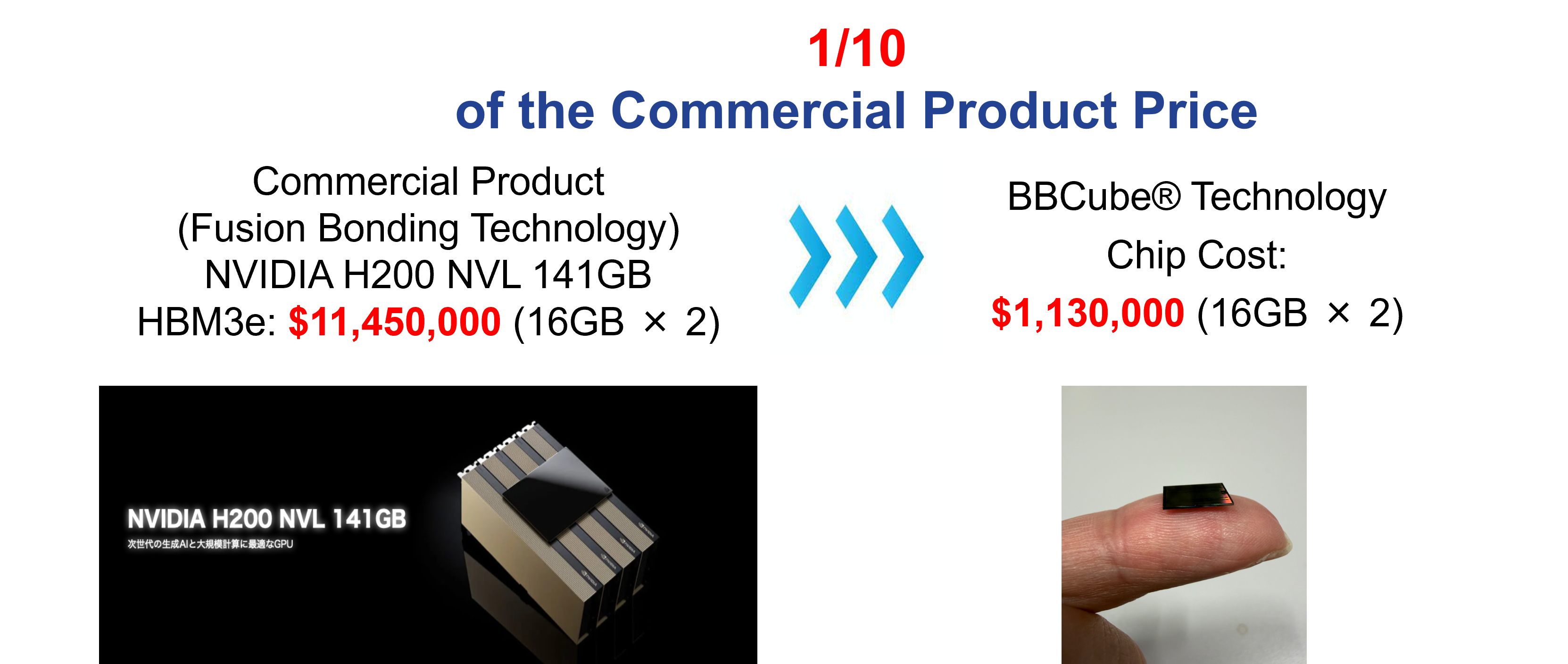
Transforming the Economic Landscape of AI Hardware
BBCube fundamentally redefines the economic landscape of next-generation AI hardware.
◆ Potential to reduce chip costs to approximately 1/10 compared to equivalent solutions.
◆ Increasing rack density.
◆ Lowering cooling infrastructure costs.
◆ Achieving superior energy efficiency (Performance-per-Watt) for hyperscale AI deployments.
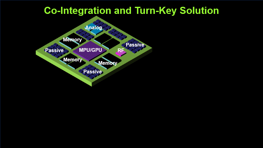
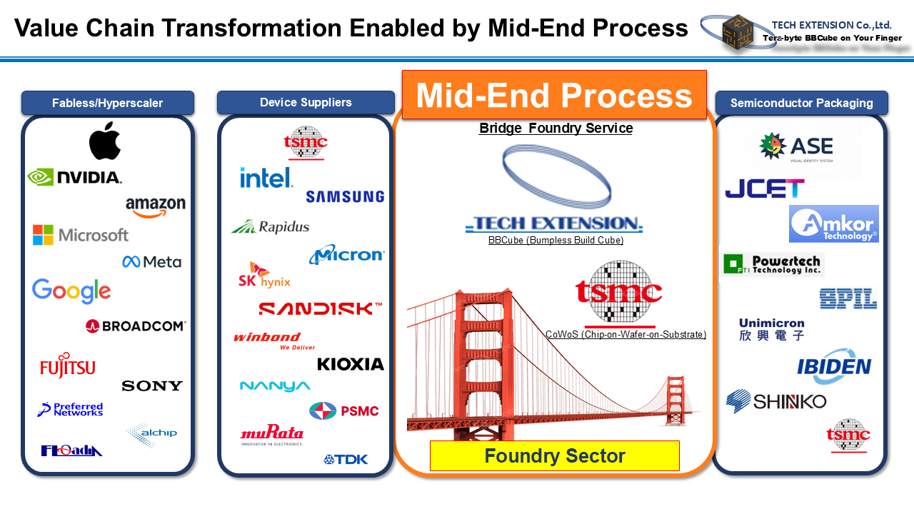
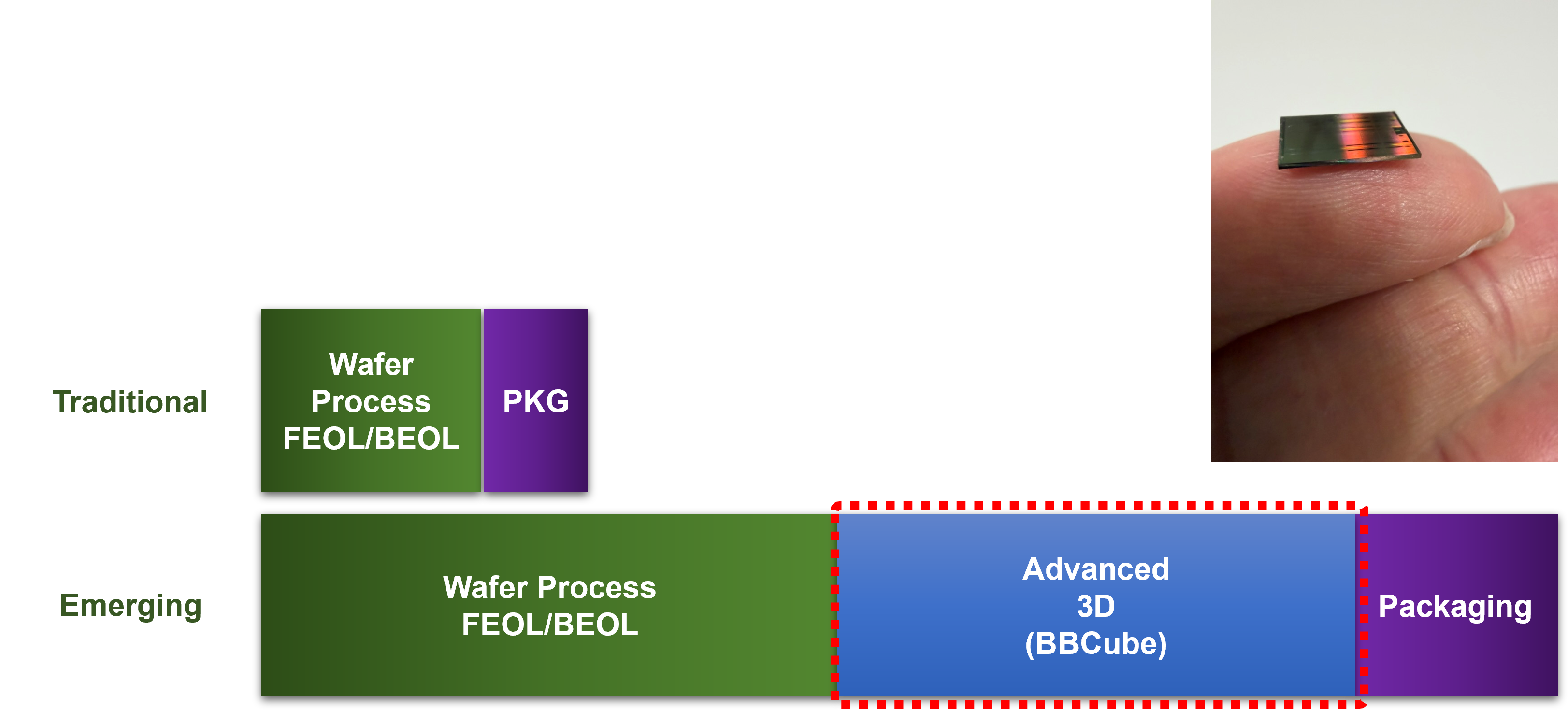
A New Industrial Layer : The Mid-end Integration Platform
In the rapidly evolving semiconductor technology stack, BBCube introduces a new industrial layer: a scalable, mid-end integration platform designed for heterogeneous AI chips.
[Conventional Structure]: FEOL → BEOL → Packaging
[New Structure]: FEOL → BEOL → Mid-end 3D Integration → Packaging
Complementary Technologies & Solutions